Handlekurv
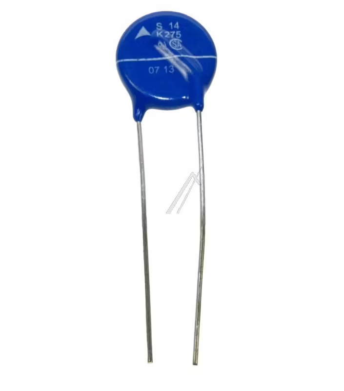
Handlekurven er tom, men det trenger den ikke å være
Handlekurven er tom, men det trenger den ikke å være
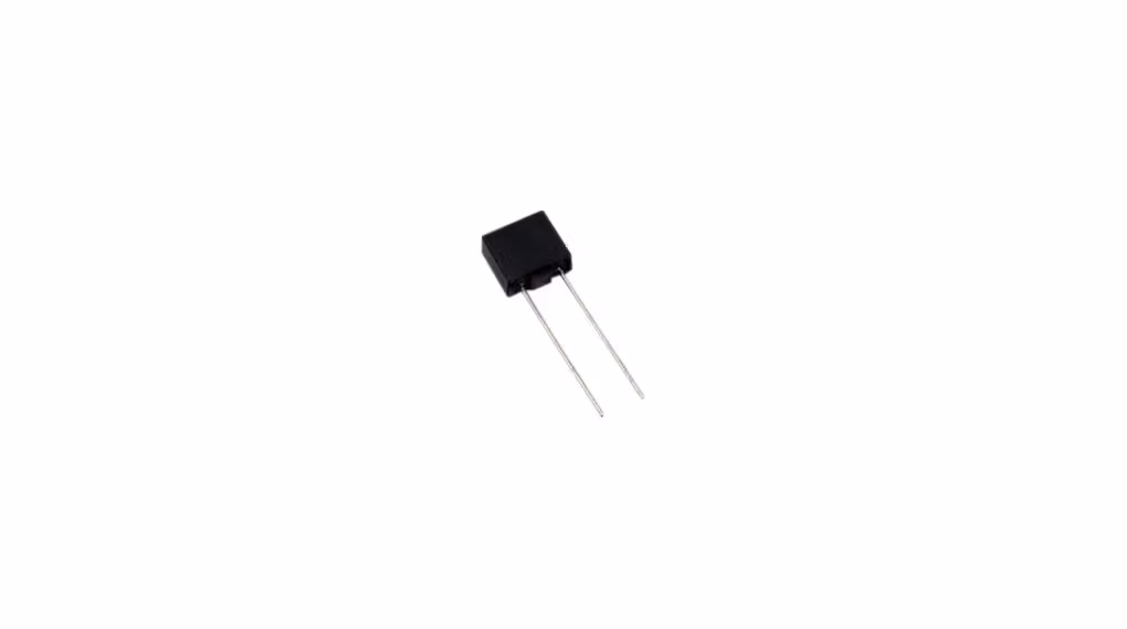
Vanlig mosfet på de fleste bærbare datmaskiner som er en vanlig komponent som tar kveld.
Symbol Min Typ Max Units
BVDSS 30 36.7 V
VDS=30V, VGS=0V 1
TJ=55°C 5
IGSS 100 nA
VGS(th) Gate Threshold Voltage 1.3 1.8 2.5 V
ID(ON) 130 A
4.5 5.5
TJ=125°C 6.8 8.2
6 7.5 mW
gFS 53 S
VSD 0.7 1 V
IS 40 A
Ciss 1930 2300 pF
Coss 290 pF
Crss 230 pF
Rg 0.7 1.4 2.1 W
Qg
(10V) 37 45 nC
Qg
(4.5V) 18 nC
Qgs 4.8 nC
Qgd 11 nC
tD(on) 8.1 ns
tr 8.6 ns
tD(off) 29 ns
tf 8 ns
trr 14 17 ns
Qrr Body Diode Reverse Recovery Charge IF=20A, dI/dt=500A/ms 40 nC
Maximum Body-Diode Continuous Current
Input Capacitance
Output Capacitance
Turn-On DelayTime
DYNAMIC PARAMETERS
Turn-On Rise Time
Turn-Off DelayTime
VGS=10V, VDS=15V, RL=0.75W,
RGEN=3W
Gate resistance VGS=0V, VDS=0V, f=1MHz
Turn-Off Fall Time
Total Gate Charge
VGS=10V, VDS=15V, ID=20A
Gate Source Charge
Gate Drain Charge
Total Gate Charge
Gate-Body leakage current
Forward Transconductance
Diode Forward Voltage
RDS(ON) Static Drain-Source On-Resistance mW
IS=1A,VGS=0V
VDS=5V, ID=20A
VGS=4.5V, ID=20A
SWITCHING PARAMETERS
Electrical Characteristics (TJ=25°C unless otherwise noted)
STATIC PARAMETERS
Parameter Conditions
IDSS mA
VDS=VGS ID=250mA
VDS=0V, VGS= ±20V
Zero Gate Voltage Drain Current
Body Diode Reverse Recovery Time
Drain-Source Breakdown Voltage
On state drain current
ID=250mA, VGS=0V
VGS=10V, VDS=5V
VGS=10V, ID=20A
Reverse Transfer Capacitance
IF=20A, dI/dt=500A/ms
VGS=0V, VDS=15V, f=1MHz
A: The value of RqJA is measured with the device mounted on 1in2 FR-4 board with 2oz. Copper, in a still air environment with TA =25°C. The Power
dissipation PDSM is based on R qJA and the maximum allowed junction temperature of 150°C. The value in any given application depends on the
user's specific board design.
B. The power dissipation PD
is based on TJ(MAX)=150°C, using junction-to-case thermal resistance, and is more useful in setting the upper
dissipation limit for cases where additional heatsinking is used.
C. Repetitive rating, pulse width limited by junction temperature TJ(MAX)=150°C. Ratings are based on low frequency and duty cycles to keep initial
TJ =25°C.
D. The RqJA is the sum of the thermal impedence from junction to case RqJC and case to ambient.
E. The static characteristics in Figures 1 to 6 are obtained using <300ms pulses, duty cycle 0.5% max.
F. These curves are based on the junction-to-case thermal impedence which is measured with the device mounted to a large heatsink, assuming a
maximum junction temperature of TJ(MAX)=150°C. The SOA curve provides a single pulse rating.
G. These tests are performed with the device mounted on 1 in2 FR-4 board with 2oz. Copper, in a still air environment with TA=25°C.

34 kr

39 kr

9 kr
49 kr
50 kr


99 kr
99 kr
19 kr

19 kr

19 kr
95 kr
15 kr


